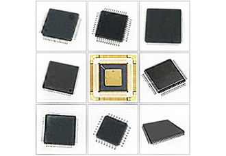
XC95288-20HQ208C
- Product Code: XC95288-20HQ208C
- Availability: In Stock
The XC95288XL is a 3.3V CPLD targeted for high-performance, low-voltage applications in leading-edge communications and computing systems. It is comprised of 16 54V18 Function Blocks, providing 6,400 usable gates with propagation delays of 6 ns.
Power Estimation
Power dissipation in CPLDs can vary substantially depending on the system frequency, design application and output loading. To help reduce power dissipation, each macrocell in a XC9500XL device may be configured for low-power mode (from the default high-performance mode). In addition, unused product-terms and macrocells are automatically deactivated by the software to further conserve power. For a general estimate of ICC, the following equation may be used:
ICC(mA) = MCHS(0.175*PTHS + 0.345) + MCLP(0.052*PTLP
+ 0.272) + 0.04 * MCTOG(MCHS +MCLP)* f
where:
MCHS = # macrocells in high-speed configuration
PTHS = average number of high-speed product terms per macrocell
MCLP = # macrocells in low power configuration
PTLP = average number of low power product terms per macrocell
f = maximum clock frequency
MCTOG = average % of flip-flops toggling per clock (~12%)
This calculation was derived from laboratory measurements of an XC9500XL part filled with 16-bit counters and allowing a single output (the LSB) to be enabled. The actual ICC value varies with the design application and should be verified during normal system operation. 288 macrocells with 6,400 usable gates
Available in small footprint packages
144-pin TQFP (117 user I/O pins)
208-pin PQFP (168 user I/O pins)
280-pin CSP (192 user I/O pins)
256-pin FBGA (192 user I/O pins)
Optimized for high-performance 2.5V systems
Low power operation
Multi-voltage operation
Advanced system features
In-system programmable
Four separate output banks
Superior pin-locking and routability with Fast CONNECT™ II switch matrix
Extra wide 54-input Function Blocks
Up to 90 product-terms per macrocell with individual product-term allocation
Local clock inversion with three global and one product-term clocks
Individual output enable per output pin
Input hysteresis on all user and boundary-scan pin inputs
Bus-hold ciruitry on all user pin inputs
Full IEEE Standard 1149.1 boundary-scan (JTAG)
Fast concurrent programming
Slew rate control on individual outputs
Enhanced data security features
Excellent quality and reliability
20 year data retention
ESD protection exceeding 2,000V

