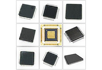
XC95144-15PQ100C
- Product Code: XC95144-15PQ100C
- Availability: In Stock
Features
• High-performance
- 5 ns pin-to-pin logic delays on all pins
- fCNT to 125 MHz
• Large density range
- 36 to 288 macrocells with 800 to 6,400 usable gates
• 5V in-system programmable
- Endurance of 10,000 program/erase cycles
- Program/erase over full commercial voltage and temperature range
• Enhanced pin-locking architecture
• Flexible 36V18 Function Block
- 90 product terms drive any or all of 18 macrocells within Function Block
- Global and product term clocks, output enables, set and reset signals
- Extensive IEEE Std 1149.1 boundary-scan (JTAG) support
- Programmable power reduction mode in each macrocell
- Slew rate control on individual outputs
- User programmable ground pin capability
- Extended pattern security features for design protection
- High-drive 24 mA outputs
- 3.3V or 5V I/O capability
- Advanced CMOS 5V FastFLASH™ technology
- Supports parallel programming of multiple XC9500 devices
Description
The XC9500 CPLD family provides advanced in-system programming and test capabilities for high performance, general purpose logic integration. All devices are in-system programmable for a minimum of 10,000 program/erase cycles. Extensive IEEE 1149.1 (JTAG) boundary-scan support is also included on all family members.
As shown in Table 1, logic density of the XC9500 devices ranges from 800 to over 6,400 usable gates with 36 to 288 registers, respectively. Multiple package options and associated I/O capacity are shown in Table 2. The XC9500 family is fully pin-compatible allowing easy design migration across multiple density options in a given package footprint.
The XC9500 architectural features address the requirements of in-system programmability. Enhanced pin-locking capability avoids costly board rework. An expanded JTAG instruction set allows version control of programming patterns and in-system debugging. In-system programming throughout the full device operating range and a minimum of 10,000 program/erase cycles provide worry-free reconfigurations and system field upgrades.
Advanced system features include output slew rate control and user-programmable ground pins to help reduce system noise. I/Os may be configured for 3.3V or 5V operation. All outputs provide 24 mA drive.144 macrocells with 3,200 usable gates
Available in small footprint packages
100-pin TQFP (81 user I/O pins)
144-pin TQFP (117 user I/O pins)
144-pin CSP (117 user I/O pins)
Optimized for high-performance 2.5V systems
Low power operation
Multi-voltage operation
Advanced system features
In-system programmable
Two separate output banks
Superior pin-locking and routability with Fast CONNECT™ II switch matrix
Extra wide 54-input Function Blocks
Up to 90 product-terms per macrocell with individual product-term allocation
Local clock inversion with three global and one product-term clocks
Individual output enable per output pin
Input hysteresis on all user and boundary-scan pin inputs
Bus-hold ciruitry on all user pin inputs
Full IEEE Standard 1149.1 boundary-scan (JTAG)
Fast concurrent programming
Slew rate control on individual outputs
Enhanced data security features
Excellent quality and reliability
20 year data retention
ESD protection exceeding 2,000V

