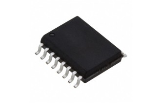
S25FL032P0XMFI001
- Product Code: S25FL032P0XMFI001
- Availability: In Stock
General Description
The S25FL032P is a 3.0 Volt (2.7V to 3.6V), single-power-supply Flash memory device. The device consists of 64 uniform 64 KB sectors with the two (Top or Bottom) 64 KB sectors further split up into thirty-two 4KB sub sectors. The S25FL032P device is fully backward compatible with the S25FL032A device.
The device accepts data written to SI (Serial Input) and outputs data on SO (Serial Output). The devices are designed to be programmed in-system with the standard system 3.0-volt VCC supply.
Distinctive Characteristics
Architectural Advantages
■ Single power supply operation
– Full voltage range: 2.7 to 3.6V read and write operations
■ Memory architecture
– Uniform 64 KB sectors
– Top or bottom parameter block (Two 64-KB sectors (top or
bottom) broken down into sixteen 4-KB sub-sectors each)
– 256-byte page size
– Backward compatible with the S25FL032A device
■ Program
– Page Program (up to 256 bytes) in 1.5 ms (typical)
– Program operations are on a page by page basis
– Accelerated programming mode via 9V W#/ACC pin
– Quad Page Programming
■ Erase
– Bulk erase function
– Sector erase (SE) command (D8h) for 64 KB sectors
– Sub-sector erase (P4E) command (20h) for 4 KB sectors
– Sub-sector erase (P8E) command (40h) for 8 KB sectors
■ Cycling endurance
– 100,000 cycles per sector typical
■ Data retention
– 20 years typical
■ Device ID
– JEDEC standard two-byte electronic signature
– RES command one-byte electronic signature for backward
compatibility
■ One time programmable (OTP) area for permanent, secure
identification; can be programmed and locked at the factory
or by the customer
■ CFI (Common Flash Interface) compliant: allows host system
to identify and accommodate multiple flash devices
■ Process technology
– Manufactured on 0.09 µm MirrorBit® process technology
■ Package option
– Industry Standard Pinouts
– 8-pin SO package (208 mils)
– 16-pin SO package (300 mils)
– 8-contact USON package (5 x 6 mm)
– 8-contact WSON package (6 x 8 mm)
– 24-ball BGA 6 x 8 mm package, 5 x 5 pin configuration
– 24-ball BGA 6 x 8 mm package, 6 x 4 pin configuration
Performance Characteristics
■ Speed
– Normal READ (Serial): 40 MHz clock rate
– FAST_READ (Serial): 104 MHz clock rate (maximum)
– DUAL I/O FAST_READ: 80 MHz clock rate or
20 MB/s effective data rate
– QUAD I/O FAST_READ: 80 MHz clock rate or
40 MB/s effective data rate
■ Power saving standby mode
– Standby Mode 80 µA (typical)
– Deep Power-Down Mode 3 µA (typical)
Memory Protection Features
■ Memory protection
– W#/ACC pin works in conjunction with Status Register Bits to
protect specified memory areas
– Status Register Block Protection bits (BP2, BP1, BP0) in status

