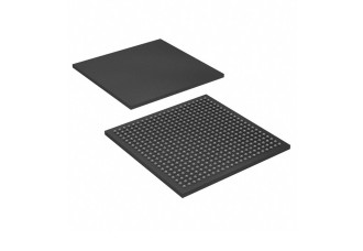
EP2C15AF484C8N
- Product Code: EP2C15AF484C8N
- Availability: In Stock
Introduction
Following the immensely successful first-generation Cyclone® device family, Altera® Cyclone II FPGAs extend the low-cost FPGA density range to 68,416 logic elements (LEs) and provide up to 622 usable I/O pins and up to 1.1 Mbits of embedded memory. Cyclone II FPGAs are manufactured on 300-mm wafers using TSMCs 90-nm low-k dielectric process to ensure rapid availability and low cost. By minimizing silicon area, Cyclone II devices can support complex digital systems on a single chip at a cost that rivals that of ASICs. Unlike other FPGA vendors who compromise power consumption and performance for low-cost, Altera’s latest generation of low-cost FPGAs—Cyclone II FPGAs, offer 60% higher performance and half the power consumption of competing 90-nm FPGAs. The low cost and optimized feature set of Cyclone II FPGAs make them ideal solutions for a wide array of automotive, consumer, communications, video processing, test and measurement, and other end-market solutions. Reference designs, system diagrams, and IP, found at www.altera.com, are available to help you rapidly develop complete end-market solutions using Cyclone II FPGAs.
Features
The Cyclone II device family offers the following features:
■ High-density architecture with 4,608 to 68,416 LEs
● M4K embedded memory blocks
● Up to 1.1 Mbits of RAM available without reducing available
logic
● 4,096 memory bits per block (4,608 bits per block including 512
parity bits)
● Variable port configurations of ×1, ×2, ×4, ×8, ×9, ×16, ×18, ×32,
and ×36
● True dual-port (one read and one write, two reads, or two
writes) operation for ×1, ×2, ×4, ×8, ×9, ×16, and ×18 modes
● Byte enables for data input masking during writes
● Up to 260-MHz operation
■ Embedded multipliers
● Up to 150 18- × 18-bit multipliers are each configurable as two
independent 9- × 9-bit multipliers with up to 250-MHz
performance
● Optional input and output registers
■ Advanced I/O support
● High-speed differential I/O standard support, including LVDS,
RSDS, mini-LVDS, LVPECL, differential HSTL, and differential
SSTL
● Single-ended I/O standard support, including 2.5-V and 1.8-V,
SSTL class I and II, 1.8-V and 1.5-V HSTL class I and II, 3.3-V PCI
and PCI-X 1.0, 3.3-, 2.5-, 1.8-, and 1.5-V LVCMOS, and 3.3-, 2.5-,
and 1.8-V LVTTL
● Peripheral Component Interconnect Special Interest Group (PCI
SIG) PCI Local Bus Specification, Revision 3.0 compliance for 3.3-V
operation at 33 or 66 MHz for 32- or 64-bit interfaces
● PCI Express with an external TI PHY and an Altera PCI Express
×1 Megacore® function
● 133-MHz PCI-X 1.0 specification compatibility
● High-speed external memory support, including DDR, DDR2,
and SDR SDRAM, and QDRII SRAM supported by drop in
Altera IP MegaCore functions for ease of use
● Three dedicated registers per I/O element (IOE): one input
register, one output register, and one output-enable register
● Programmable bus-hold feature
● Programmable output drive strength feature
● Programmable delays from the pin to the IOE or logic array
● I/O bank grouping for unique VCCIO and/or VREF bank
settings
● MultiVolt™ I/O standard support for 1.5-, 1.8-, 2.5-, and
3.3-interfaces
● Hot-socketing operation support
● Tri-state with weak pull-up on I/O pins before and during
configuration
● Programmable open-drain outputs
● Series on-chip termination support

