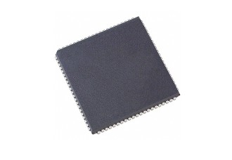
EPF8636ALC84-3
- Product Code: EPF8636ALC84-3
- Availability: In Stock
General Description
Altera’s Flexible Logic Element MatriX (FLEX®) family combines the benefits of both erasable programmable logic devices (EPLDs) and fieldprogrammable gate arrays (FPGAs). The FLEX 8000 device family is ideal for a variety of applications because it combines the fine-grained architecture and high register count characteristics of FPGAs with the high speed and predictable interconnect delays of EPLDs. Logic is implemented in LEs that include compact 4-input look-up tables (LUTs) and programmable registers. High performance is provided by a fast, continuous network of routing resources.
Features...
■ Low-cost, high-density, register-rich CMOS programmable logic
device (PLD) family (see Table 1)
– 2,500 to 16,000 usable gates
– 282 to 1,500 registers
■ System-level features
– In-circuit reconfigurability (ICR) via external configuration
devices or intelligent controller
– Fully compliant with the peripheral component interconnect
Special Interest Group (PCI SIG) PCI Local Bus Specification,
Revision 2.2 for 5.0-V operation
– Built-in Joint Test Action Group (JTAG) boundary-scan test (BST)
circuitry compliant with IEEE Std. 1149.1-1990 on selected devices
– MultiVoltTM I/O interface enabling device core to run at 5.0 V,
while I/O pins are compatible with 5.0-V and 3.3-V logic levels
– Low power consumption (typical specification is 0.5 mA or less in
standby mode)
■ Flexible interconnect
– FastTrack® Interconnect continuous routing structure for fast,
predictable interconnect delays
– Dedicated carry chain that implements arithmetic functions such
as fast adders, counters, and comparators (automatically used by
software tools and megafunctions)
– Dedicated cascade chain that implements high-speed, high-fan-in
logic functions (automatically used by software tools and
megafunctions)
– Tri-state emulation that implements internal tri-state nets
■ Powerful I/O pins
■ Programmable output slew-rate control reduces switching noise
■ Peripheral register for fast setup and clock-to-output delay
■ Fabricated on an advanced SRAM process
■ Available in a variety of packages with 84 to 304 pins (see Table 2)
■ Software design support and automatic place-and-route provided by
the Altera® MAX+PLUS® II development system for Windows-based
PCs, as well as Sun SPARCstation, HP 9000 Series 700/800, and IBM
RISC System/6000 workstations
■ Additional design entry and simulation support provided by EDIF
2 0 0 and 3 0 0 netlist files, library of parameterized modules (LPM),
Verilog HDL, VHDL, and other interfaces to popular EDA tools from
manufacturers such as Cadence, Exemplar Logic, Mentor Graphics,
OrCAD, Synopsys, Synplicity, and Veribest

