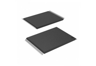
JS28F640J3F75A
- Product Code: JS28F640J3F75A
- Availability: In Stock
Introduction
This document contains information pertaining to the Numonyx® Embedded Flash Memory (J3 65 nm) Single Bit per Cell (SBC) device features, operation, and specifications.
Unless otherwise indicated throughout the rest of this document, the Numonyx® Embedded Flash Memory (J3 65 nm) Single Bit per Cell (SBC) device is referred to as J3 65 nm SBC.
The J3 65 nm SBC device provides improved mainstream performance with enhanced security features, taking advantage of the high quality and reliability of the NOR-based 65 nm technology. Offered in 128-Mbit, 64-Mbit, and 32-Mbit densities, the J3 65 nm SBC device brings reliable, low-voltage capability (3 V read, program, and erase) with high speed, low-power operation. The J3 65 nm SBC device takes advantage of proven manufacturing experience and is ideal for code and data applications where high density and low cost are required, such as in networking, telecommunications, digital set top boxes, audio recording, and digital imaging. Numonyx Flash Memory components also deliver a new generation of forward-compatible software support. By using the Common Flash Interface (CFI) and Scalable Command Set (SCS), customers can take advantage of density upgrades and optimized write capabilities of future Numonyx Flash Memory devices.
Product Features
■ Architecture
— Symmetrical 128-KB blocks
— 128 Mbit (128 blocks)
— 64 Mbit (64 blocks)
— 32 Mbit (32 blocks)
— Blank Check to verify an erased block
■ Performance
— Initial Access Speed: 75ns
— 25 ns 8-word Asynchronous page-mode
reads
— 256-Word write buffer for x16 mode, 256-
Byte write buffer for x8 mode;
1.41 µs per Byte Effective programming
time
■ System Voltage
— VCC = 2.7 V to 3.6 V
— VCCQ = 2.7 V to 3.6 V
■ Packaging
— 56-Lead TSOP
— 64-Ball Easy BGA package
■ Security
— Enhanced security options for code
protection
— Absolute protection with VPEN = Vss
— Individual block locking
— Block erase/program lockout during power
transitions
— Password Access feature
— One-Time Programmable Register:
64 OTP bits, programmed with unique
information by Numonyx
64 OTP bits, available for customer
programming
■ Software
— Program and erase suspend support
— Numonyx® Flash Data Integrator (FDI)
— Common Flash Interface (CFI) Compatible
— Scalable Command Set
■ Quality and Reliability
— Operating temperature:
-40 °C to +85 °C
— 100K Minimum erase cycles per block
— 65 nm Flash Technology
— JESD47E Compliant

